Infineon opens high-tech chip factory for power electronics on 300-millimetre thin wafers

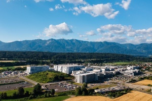
Infineon Technologies AG opened its high-tech chip factory for power electronics on 300-millimetre thin wafers at its Villach site in Austria under the motto “Ready for Mission Future.” At 1.6 billion euros, the investment made by the semiconductor group represents such projects in the microelectronics sector in Europe.
The Villach site is modern fabs and was opened by Infineon CEO Reinhard Ploss, Infineon Austria CEO Sabine Herlitschka along with EU commissioner Thierry Breton and Austrian chancellor Sebastian Kurz.
Infineon set the stage for long-term, profitable growth based on energy efficiency and CO 2 reduction at an early stage and announced the construction of the chip factory for power electronics (“energy-saving chips”) in 2018. “The new fab is a milestone for Infineon, and its opening is very good news for our customers,” Ploss says. “The timing to create new capacity in Europe could not be better, given the growing global demand for power semiconductors.
The last few months have clearly shown how essential microelectronics are in virtually every area of life. Given the accelerated pace of digitalisation and electrification, we expect demand for power semiconductors to continue to grow in the coming years. The additional capacities will help us serve our customers worldwide even better, including long term.”
The global chip-market situation clearly shows how important investments in innovative technologies are for the future. Today, microelectronics is the dominant technology on which all other developments, systems and technologies in the area of digitalisation are based. With the expansion of its production facilities, Infineon is setting an industrial policy milestone in terms of supply security for both European industry and the global market.
First products are currently being shipped
After three years of preparation and construction, the factory was commissioned at the beginning of August, three months ahead of schedule. The first wafers will leave the Villach plant this week. In the first stage of expansion, the chips will primarily be used to meet demand from the automotive industry, data centres and renewable energy generation of solar and wind power. On the group level, the new factory will give Infineon additional sales potential of around two billion euros per year.
The semiconductors produced in Villach will be used in numerous applications. As a result, the new factory will enable Infineon to serve the growing market for power semiconductors in electric cars, data centres as well as solar and wind energy. Arithmetically speaking, the annual capacity planned for industrial semiconductors is sufficient to equip solar systems producing a total of around 1,500 TWh of electricity roughly three times the annual power consumption in Germany.
At the opening, Kurz underscored the new chip factory’s significance, including to his own country. “The Infineon site in Villach is an absolute success story,” he says. “The new chip factory is an economic and technological lighthouse project for all of Austria. I would like to thank all of those responsible for their commitment to our country, which will create an additional 400 jobs. The immense investment of 1.6 billion euros shows that Austria, as a business and technology location, offers excellent framework conditions and the employee know-how that is needed to make them happen. We in the federal government want to continue to invest massively in digitisation in order to position ourselves in the best possible way in global competition.”
Sabine Herlitschka, the CEO of Infineon Technologies Austria AG, says, “With this investment, Infineon has demonstrated that it is also possible to build attractive production sites in Europe in the highly competitive microelectronics sector. We are setting new standards with this investment. The energy-saving chips from Villach will become important core elements for the energy transition. We are thus making a relevant contribution to the European Green Deal and beyond. We are ‘Ready for Mission Future.’”
Energy-saving chips for ‘green’ products

Infineon’s products have been contributing to higher energy efficiency and thus to climate protection for years. Infineon’s Villach site plays a crucial role in these solutions as it serves as the global centre of expertise for power electronics. These energy-saving chips switch electricity intelligently and minimise the carbon footprint of numerous applications. They reduce energy consumption in household appliances, LED lighting and mobile devices.
For example, modern semiconductors can reduce the energy consumption of refrigerators by 40%. The energy consumption of lighting in buildings is reduced by 25%. With the products manufactured in the new production facility, more than 13 million tons of CO 2 can be avoided thanks to the product mix in Villach. This equals the amount of CO 2 that is produced by more than 20 million people living in Europe.
Energy-efficient factory
During the construction of the factory, the company paid particular attention to ways that could further improve its energy balance sheet: 80% of the site’s heating requirements will be covered by intelligently recycling the waste heat of the cooling systems, and around 20,000 tons of CO 2 will be avoided each year. The extensive use of exhaust air purification systems will cut direct emissions to virtually zero.
Another milestone in terms of sustainable production and circular economy is the production and recycling of green hydrogen. The hydrogen required as a process gas in production will be produced directly on site in Villach from renewable energy sources starting at the beginning of 2022. This will eliminate CO 2 emissions during the original production and transport. This green hydrogen will be recycled after use in chip production and used to fuel public transportation buses. This project of dual use of green hydrogen is unique in Europe. With the help of these and other measures, the site will make enable the Infineon Group to take a huge stride forward in its effort to become carbon neutral by 2030.
Ultra-modern chip factory links two sites in Europe to form a mega-factory
The new chip factory has about 60,000 m² of gross floor space. Production will be gradually ramped up over the next four to five years. More than two-thirds of the 400 additional highly qualified specialists needed to operate the factory have already been hired.
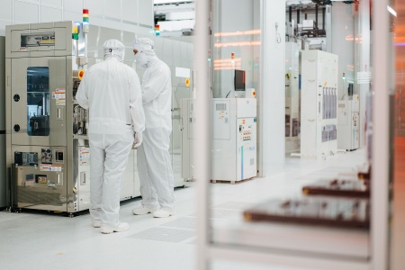
The chip factory is one of the most modern in the world and relies on full automation and digitisation. As a “learning factory,” artificial intelligence solutions will be used primarily in the area of predictive maintenance. Networked plants will know at an early stage when they need maintenance thanks to a multitude of data and simulations.
Infineon is going one step farther. Jochen Hanebeck, a member of the management board and chief operations officer of Infineon, says “Infineon now has two large power semiconductor manufacturing sites for 300-millimetre thin wafers, one in Dresden and one in Villach. Both sites are based on the same standardised production and digitisation concepts. This allows us to control the manufacturing operations at the two sites as if they were one factory. We increase productivity and create additional flexibility for our customers.
This is because we can quickly move production volumes for different products between the sites and thus respond even faster to their needs. With the virtual megafactory, Infineon is setting a new benchmark in 300-millimetre manufacturing. This makes further increases in resource and energy efficiency possible, as well as optimisation of the environmental footprint.”
Global provider of 300-millimetre thin-wafer technology, power electronics
The chips are manufactured on 300-millimetre thin wafers, which at 40 micrometres are thinner than a human hair. Villach is the Group’s centre of expertise for power semiconductors and has long been an important innovation site in Infineon’s manufacturing network. It was here that the production of power semiconductors on 300-millimetre thin wafers was developed about 10 years ago. This was then expanded to fully automated volume production at the Dresden site in recent years. The use of this technology brings significant productivity advantages due to the larger wafer diametre and reduces capital expenditure.
Comment on this article below or via Twitter @IoTGN
